岡本 明彦
東京大学
産学協創推進本部 イノベーション推進部
プログラムオフィサー
略 歴
- 【学 歴】
- 1977年
- 東京大学工学部物理工学科 卒業
- 1980年
- マサチューセッツ工科大学 Dep. of Materials Science and Engineering
研究テーマ:有機材料の物性、修士課程 修了 - 1982年
- マサチューセッツ工科大学 Dep. of Materials Science and Engineering
研究テーマ:半導体結晶成長技術、博士号取得 - 【職 歴】
- 1982-2011年
- 大手電気機器メーカの研究部門にて研究開発およびマネジメント業務に従事
在職中従事した主な業務:
(1)半導体デバイス技術の確立(結晶成長技術、プロセス技術、デバイス基礎技術等)
(2)電界放出デバイス技術の確立(冷陰極管真空デバイス及びディスプレイ技術等)
(3)半導体エレクトロニクス分野での研究企画部門従事
研究者あるいは研究管理者として国内外の大学・研究機関、関連企業との連携研究、技術移転を経験。 - 2011年から現在
- 東京大学産学協創推進本部イノベーション推進部にてプログラムオフィサーとして新規産学連携開拓/推進、コンソーシアム及びサロンの設立/運営に従事
現職においてこれまでに従事した主な事業・プロジェクト:
・アンビエント社会基盤研究会 (2010年9月~2012年4月)
・科学・技術交流サロン「宇宙利用の新しい展開」(2015年9月~2016年10月)
・レアアース泥開発推進コンソーシアム (2014年11月~)
・科学技術交流フォーラム企画・開催
-「宇宙利用の新しい展開」-衛星と応用技術による産業創生-(2014年10月)
-「社会を変えるものづくりイノベーション」-設計・製造技術の新たな挑戦- (2013年11月)
-「有機材料・有機デバイスでフロンティアを切り拓く」-革新的エネルギー・環境、医療イノベーションを創造-(2012年11月)
-「電力エネルギーにおける技術革新」東日本大地震を踏まえ加速すべき新技術(2011年10月)
- 【主要資格等】
- 放射線取扱主任者 1種(1990 年3月)
衛生管理者 1種(2005 年11月)
日商簿記検定2級、3級(1999 年12月)
- 【職務発明等】
- 平成12年度地方発明表彰 他 成立特許31件
主要論文等
1 A. Okamoto, J. Lagowski, and H. C. Gatos, Enhancement of interface stability in liquid phase electroepitaxy, J. Appl. Phys. 53, 1706 (1982)
2 A. Okamoto, S. Isozumi, J. Lagowski, and H.C. Gatos In Situ Monitoring of Liquid Phase Electroepitaxial Growth, J. Electrochem. Soc. 129, 2095 (1982)
3 A Okamoto, H. Sunakawa H. Terao and H.Watanabe, Extremely Uniform Growth of GaAs and GaAlAs by Low Pressure Metalorganic Chemical Vapor Deposition on Three-Inch GaAs Substrates, Joural of Crystal Growth 70, 140 (1984)
4 A Okamoto, Hiroshi Terao and T. Kamejima Uniform Epitaxial Growth of Modulation-Doped GaAs/Ga07Al0.3As on Three-Inch Substrate by Metalorganic Chemical Vapor Depositions, Japan Journal of Applied Physics 28, 238 (1986)
5 A. Okamoto, H.Toyoshima and K.Ohata, Strained N-Ga0.3Al0.7As/In0.23Ga0.77As/ GaAs 2DEG FET with large band offset, Gallium Arsenide Integrated Circuit (GaAsIC) Symposium, 1986Technical Digest 1986,8th Annua 8,569 (1986)
6 A. Okamoto, H.Toyoshima and K.Ohata Strained N-Ga0.3Al0.7As/InxGa1-xAs/ GaAs Modulation-Doped Structures, Japanese Journal of Applied Physics 26, 539 (1987)
7 A. Okamoto, and K.Ohata, Selectively Epitaxial Growth of InAs on GaAs by Molecular Beam Epitaxy Japanese Journal of Applied Physics 26, L1174 (1987)
8 A. Okamoto, and K.Ohata, Selectively Epitaxial Growth of gallium arsenide by Molecular Beam Epitaxy, Applied Physics Letters 51, 1512 (1987)
9 岡本 明彦 大畑 恵一MBE法を用いたGaAs,InAs選択成長電子情報通信学会 ED87-118, 49 (1987)
10 A. Okamoto, and K.Ohata, Substrate temperature lowering in GaAs selective epitaxial growth by molecular-beam epitaxy Jouranl of Applied Physics 66,3413 (1989)
11 A. Okamoto, and K.Ohata, Growth Condition Dependence for GaAs Selective Epitaxial Growth by Molecular Beam Epitaxy, Journal of Electronic Materials 18, 111 (1989)
12 A. Okamoto, Hironobu Miyamoto, HideoToyoshima, Naoki Furuhata,Kensuke Kawahara and Yasushi Shiraishi, Crystal Growth Technology for Ultrahigh-Speed Devices NEC Research & Development 33, 443 (1992)
13 A. Okamoto Material Trends in Ultra High Speed Devices, 1992 Microwave Workshops and Exhibition 1992, 387 (1992)
14 A. Okamoto, Selective epitaxial growth by molecular beam epitaxy, Semicon.Sci. Technol 8, 1011 (1993)
15 岡本 明彦、小沼 和夫、富張 美徳、伊藤 文則、岡田 裕子, カーボンナノチューブFEDの低駆動電圧化月間ディスプレイ2002 3月24日
(共 著)
1 S. Isozumi, C. J. Herman, A. Okamoto, J.Lagowski, and H. C. Gatos、A New Approach to Liquid Phase Electroepitaxy (LPEE) of III–V Compounds, J. Electrochem 128, 2220 (1981)
2 H. Toyoshima, Y. Ando, A. Okamoto and T. Itoh, New Resonant Tunneling Diode with a Deep Quantum-Well, J. J. Appl. Phys 25, L786 (1986)
3 H. Hida, A. Okamoto, H. Toyoshima and K. Ohata, A high-current drivability i-AlGaAs/n-GaAs doped-channel MIS-Like FET (DMT), Electron Device Letters, IEEE 7, 625 (1986)
4 H. Hida, A. Okamoto, H. Toyoshima, S. Tahara and K. Ohata, New high current drivability MIS-like FET's utilizing a highly doped thin GaAs channel Electron Devices, IEEE Transactions 33, 1852 (1986)
5 H. Hida, Y. Suzuki, F. Katano, H. Toyoshima, A. Okamoto and S. Kumashiro, A 760mS/mm N+self-aligned enhancement mode doped-channel MIS-like FET (DMT),Electron Devices Meeting, 1986 International 32, 759 (1986)
6 N. Hayama,, A. Okamoto, M. Madihian and K. Honjo, Submicrometer fully self-aligned AlGaAs/GaAs Heterojunction bipolar transistor Electron Device Letters, IEEE 8, 246 (1987)
7 H Hida, A. Okamoto, H. Toyoshima and K. Ohata, An investigation of i-AlGaAs/n-GaAs doped hannel MIS-like FET's (DMT's)—Properties and performance potentialities Electron Devices, IEEE Transactions 34, 1448 (1987)
8 N. Hayama, M Madihian, A. Okamoto, H. Toyoshima and K. Honjo, Fully self-aligned AlGaAs/GaAs heterojunction bipolar transistors for high-speed integrated circuits application, Electron Devices, IEEE Transactions 35, 1771 (1988)
9 N. Furuhata, H. Miyamoto, A. Okamoto, and K. Ohata, Chemical dry etching of GaAs and InP by Cl2 using a new ultrahigh-vacuum dry-etching molecular beam epitaxy system, J. Appl. Phys. 66, 3413 (1989)
10 M. Madihian, S. Tanaka, N. Hayama, A. Okamoto and K Honjo, Application of AlGaAs/GaAs HBTs to high-speed, CML logic family fabrication、Electron Devices, IEEE Transactions 36, 625 (1989)
11 Y. Suzuki, H. Hida, T. Suzaki, S. Fujita, Y. Ogawa, A. Okamoto and T. Toda, T. Nozaki, A 10-Gbit/s laser driver IC with i-AlGaAs/n-GaAs doped-channel hetero-MISFETs (DMTs), Gallium Arsenide Integrated Circuit (GaAs IC) Symposium, 1989, Technical Digest 1989.,11th Annual 11, 129 (1989)
12 H. Toyoshima, T. Anan, K. Nishi, T. Ichihashi, and A. Okamoto, Growth by molecular-beam epitaxy and characterization of (InAs)m(GaAs)m short period superlattices on InP substrates, J. Appl. Phys. 68, 1282 (1990)
13 H. Toyoshima, K. Onda, E. Mizuki, N. Samoto, M. Kuzuhara, T. Itoh, A. Okamoto, T. Anan, and T. Ichihashi, Molecular-beam epitaxial growth of InAs/GaAs superlattices on GaAs substrates and its application to a superlattice channel modulationdoped field-effect transistor, J. Appl. Phys. 69, 3941 (1991)
14 Y. Suzuki, T. Suzaki, Y. Ogawa, W. Liu, S. Fujita and A. Okamoto, Pseudomorphic 2DEG FET ICs for ultra high-speed optical communication systems with an external optical modulator Gallium Arsenide Integrated Circuit (GaAs IC) Symposium, 1991,.Technical Digest 1991.,13th Annual 213 (1991)
15 Y Shiraishi, T. Yoshida, N. Furuhata and A. Okamoto, Growth and Characterization of excellent nonalloyed ohmic contacts using graded bandgap InAs/GaAs strained-layer superlattice structures by MBE, Int. Symp. GaAs and Related Compounds 1992 639 (1992)
16 Y. Suzuki, T. Suzaki,Y. Ogawa,S. Fujita, W. Liu. And A. Okamoto, Pseudomorphic 2DEG FET IC's for 10 Gb/s optical communication systems with external optical modulation, Solid-State Circuits, IEEE Journal of 1992 27, 1342
17 二瓶 史行、佐本典彦、岡本明彦、 中村和夫、アンチドット格子におけるバリスティック伝導(社)電気学会 EFM-91-(1992)
18 H. Toyoshima, T. Niwa, J. Yamazaki and A. Okamoto, In surface segregation and growth-mode transition during InGaAs growth by molecular-beam epitaxy, Applied Physics Letters 63, 821 (1993)
19 H. Toyoshima, T. Niwa, J. Yamazaki and A.Okamoto, Suppression of In surface segregation and growth of modulation-doped N-AlGaAs/InGaAs/GaAs structures with a high In composition by molecular beam epitaxy, Journal of Applied Physics 75, 3908 (1994)
20 Y. Shiraishi, N. Furuhata, and A. Okamoto, Influence of metal/n-InAs/interlayer /n-GaAs structure on nonalloyed ohmic contact resistance, J. Appl. Phys. 76, 5099 (1994)
21 F. Ito, K. Konuma, A. Okamoto, A. Yano and S. Miyano, Effects of thermal annealing on emission characteristics and surface properties of field emitter arrays, J. Appl. Phys. 82, 6267 (1997)
22 H. Takemura, N. Furutake, M. Nisimura, S. Tsuida, M. Yoshiki,, A. Okamoto and S. Miyano, Fully large-scale integration-process -compatible Si field emitter technology with high controllability of emitter height and sharpness, J. Vac. Sci. Technol. B 15, 503 (1997)
23 H. Imura, S. Tsuida, M. Takahasi., A. Okamoto, H. Makishima, and S. Miyano, Electron gun design for traveling wave tubes (TWTs) using a field emitter array (FEA) cathode Electron Devices Meeting, 1997.IEDM '97, Technical Digest., International 721 (1997)
24 H. Takemura, Y. Tomihari, N. Furutake, F. Matsuno, M. Yoshiki, N. Takada, A. Okamoto and S. Miyano, A novel vertical current limiter fabricated with a deep trench forming technology for highly reliable field emitter arrays, Electron Devices Meeting, 1997. IEDM '97 Technical Digest., International 709 (1997)
25 H. Makishima, H. Imura, M. Takahashi, H. Fukui and A. Okamoto, Remarkable improvements of microwave electron tubes through the development of the cathode materials, Vacuum Microelectronics Conference, 1997., Technical Digest., 1997, 10th International 194 (1997)
26 F. Ito, K. Konuma, A. Okamoto and A. Yano, Effects of thermal annealing on emission characteristics and emitter surface properties of a Spindt-type field emission cathode Vacuum, Microelectronics Conference, 1997., Technical Digest., 1997, 10th International 68 (1997)
27 F. Ito, K. Konuma, A. Okamoto and A. Yano, Effects of thermal annealing on emission characteristics and emitter surface properties of a Spindt-type field emission cathode, J. Vac. Sci. Technol. B 16 783 (1998)
28 H. Takemura, M. Yoshiki, N. Furutake, Y. Tomihari, A. Okamoto and S. Miyano,, Si field emitter array with 90-nm-diameter gate holes, Electron Devices Meeting, 1998. IEDM '98, Technical Digest.,International 859 (1998)
29 M. Yoshiki, N. Furutake, H. Takemura, A.Okamoto and S. Miyano, A novel field emitter array technology for subhalfmicron diameter gates, J. Vac. Sci. Technol. B 17, 567 (1999)
30 H. Makishima, S. Miyano, H. Imurat, J. Matsuoka, H. Takemura and A. Okamoto, Design and performance of traveling-wave tubes using field emitter array cathodes,Appl. Surf. Sci. 146, 230 (1999)
31 K. Konuma, Y. Okada, A. Okamoto, Y. Tomihari and S. Miyano, A field-emitter-array cathode-ray tube (FEA-CRT) J. Soc. Inf. Display 8, 233, (2000)
32 F. Ito, Y. Tomihari, Y. Okada, K. Konuma and A. Okamoto, Extremely Low-Voltage triode Flat Panel display using Carbon Nanotube, IDW'00 1177 (2000)
33 Y. Tomihari, F. Ito, Y. Okada, K. Konuma and A. Okamoto, Multi-Layered Triode(MLT) Developed for CNTFED, IDW'01 1213 (2001)
34 F. Ito, K. Konuma and A. Okamoto, Electron emission from single-walled carbon nanotubes with sharpened bundles, J. Appl. Phys. 89, 8141(2001)
35 F. Ito, Y. Tomihari, Y. Okada. K. Konuma and A. Okamoto, Carbon-nanotube-based triode-field-emission displays using gated emitter structure, Electron Device Letters, IEEE 22, 426 (2001)
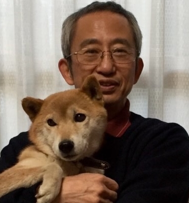
趣味 詩音ちゃんと詩音丸くんとのお散歩